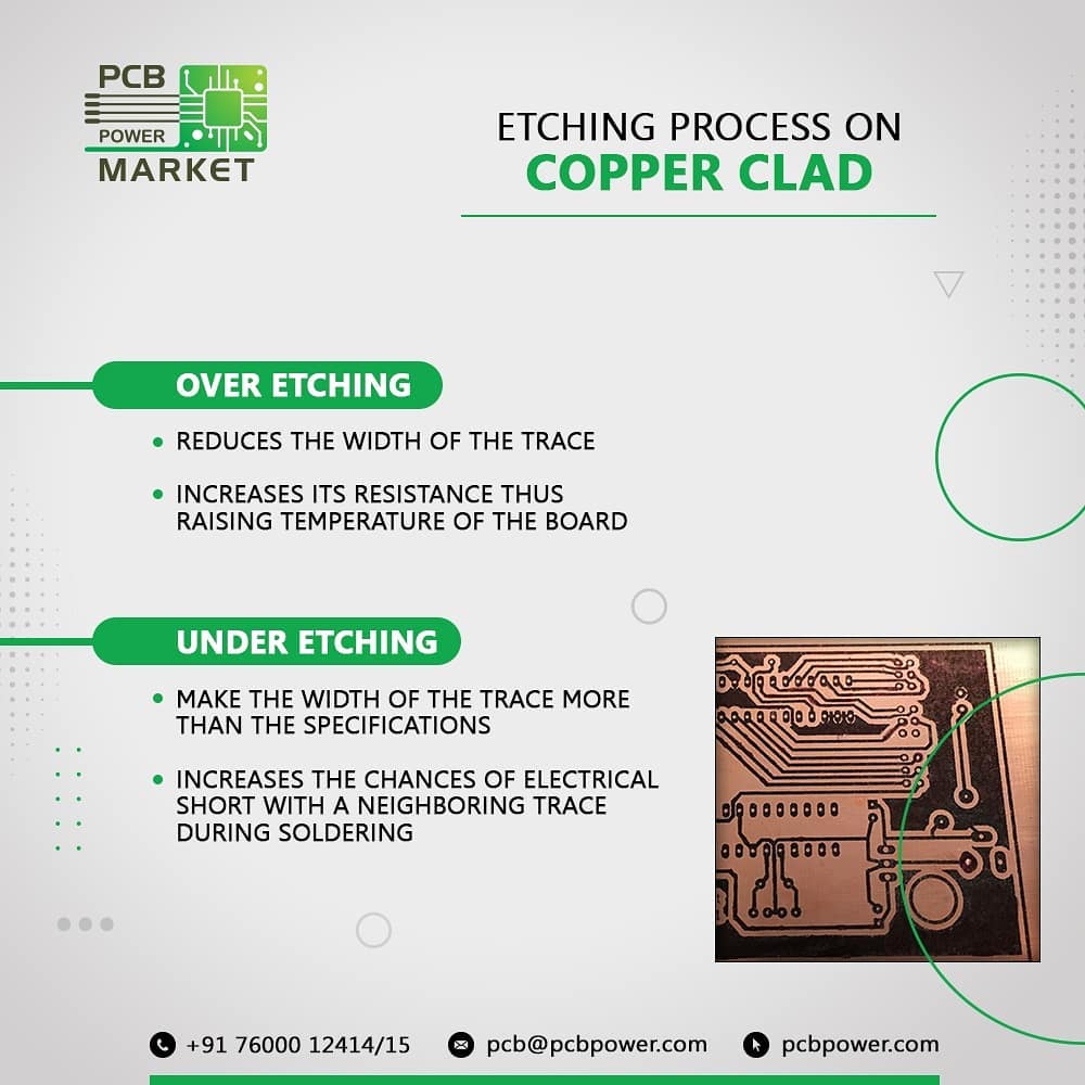
The etching process defines the quality of the copper traces. The weight of copper of the copper clad defines the thickness of the copper trace, but the etching process defines its width.
Enquire now!
For further details, visit - https://www.pcbpower.com
#BePCBWise #MakeInIndia #SupportMakeInIndia #pcbmanufacturers #electronics #pcbelectronics #pcbdesigners #PCBPowerMarket #pcbassembly #pcbmanufacturing #pcbdesign #pcb
The etching process defines the quality of the copper traces. The weight of copper of the copper clad defines the thickness of the copper trace, but the etching process defines its width. Enquire now! For further details, visit - https://www.pcbpower.com #BePCBWise #MakeInIndia #SupportMakeInIndia #pcbmanufacturers #electronics #pcbelectronics #pcbdesigners #PCBPowerMarket #pcbassembly #pcbmanufacturing #pcbdesign #pcb
May 29, 2021