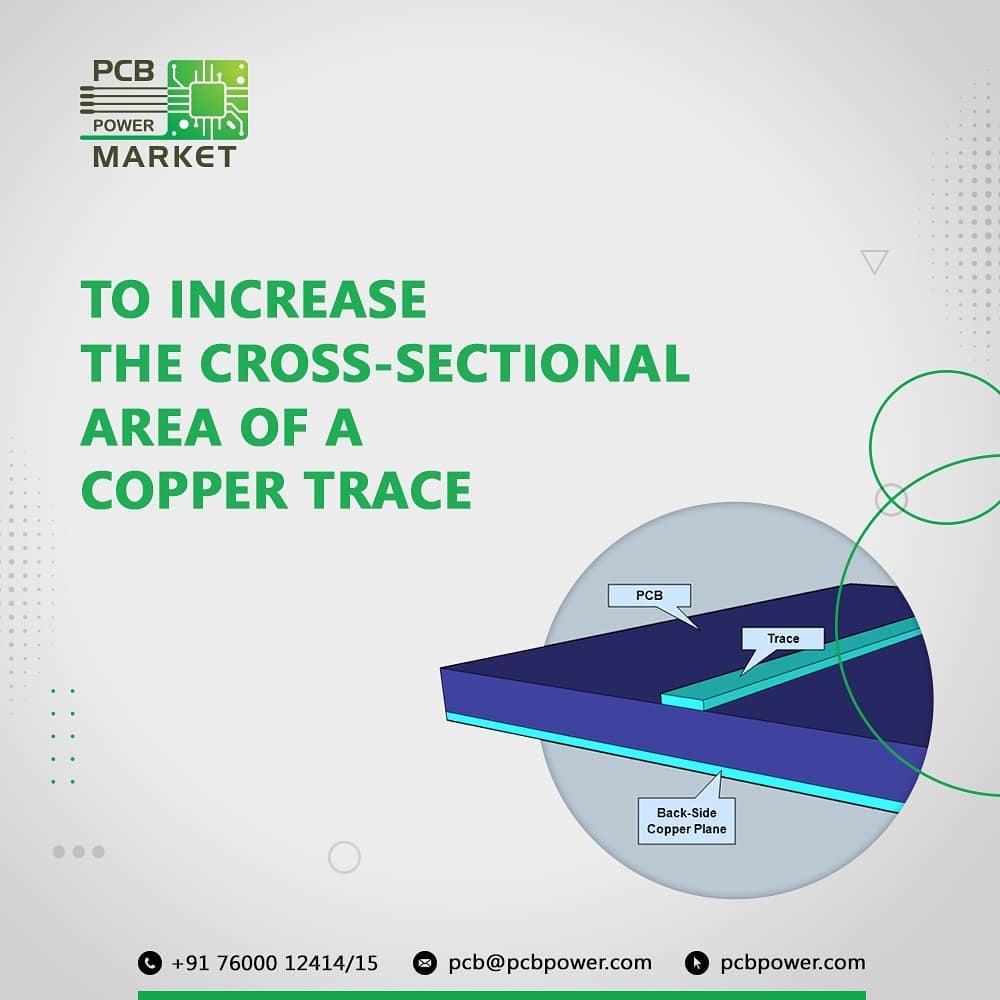
If the designer has ample space on the board to increase the width of the trace, they can continue using the standard copper weight of 35-70 microns (1 to 2 oz). By increasing the width of the copper trace, the designer effectively increases its cross-sectional area, reducing its resistance to the increased current flow.
If the size of the board restricts the designer from increasing the width of the trace to the desired extent, the designer can take recourse to increasing the number of layers or increasing the copper weight.
To know more - https://www.pcbpower.com/blog.../importance_of_pcb_thickness
#BePCBWise #MakeInIndia #SupportMakeInIndia #pcbmanufacturers #electronics #pcbelectronics #pcbdesigners #PCBPowerMarket #pcbassembly #pcbmanufacturing #pcbdesign #pcb
If the designer has ample space on the board to increase the width of the trace, they can continue using the standard copper weight of 35-70 microns (1 to 2 oz). By increasing the width of the copper trace, the designer effectively increases its cross-sectional area, reducing its resistance to the increased current flow. If the size of the board restricts the designer from increasing the width of the trace to the desired extent, the designer can take recourse to increasing the number of layers or increasing the copper weight. To know more - https://www.pcbpower.com/blog.../importance_of_pcb_thickness #BePCBWise #MakeInIndia #SupportMakeInIndia #pcbmanufacturers #electronics #pcbelectronics #pcbdesigners #PCBPowerMarket #pcbassembly #pcbmanufacturing #pcbdesign #pcb